PHYSICAL ONLY CELLS
- These cells are not present in the design netlist. If the name of a cell is not present in the current design, it will consider as physical only cells. they do not appear on timing paths reports, they are typically invented for finishing the chip.
 |
| fig: TAP Cells and END CAP Cells |
Tap cells :
- A tap cell is a special non-logic cell with a well tie, substrate tie, or both.
- Tap cells are placed in the regular intervals in standard cell row and distance between two tap cells given in the design rule manual.
- These cells are typically used when most or all of the standard cells in the library contain no substrate or well taps.
- Generally, the design rules specify the maximum distance allowed between every transistor in a standard cell and a well or substrate tap.
- Before global placement (during the floorplanning stage), you can insert tap cells in the block to form a two-dimensional array structure to ensure that all standard cells placed subsequently comply with the maximum diffusion-to-tap distance limit.
- Physical only cells which helps to tie substrate and N-Wells to VDD and GND levels, and thus avoids latchup possibiities.
What is Latch - up problem ?
- It is the condition when low impedance path gets formed between VDD and GND terminal and there is direct current flow from VDD to GND which might result in a complete failure of chip.
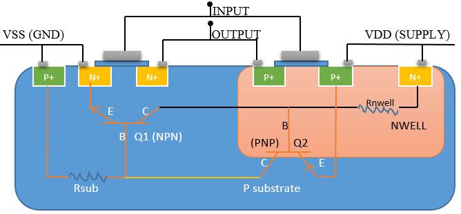
- While the formation of CMOS INVERTER we saw the formation of PN junctions and because of these PN junctions there may be formation of parasitics elements like diode and transistors.
 |
| FIG: latch-up phenomenon |
- Transistors Q1(NPN) and Q2(PNP) are parasitics transistors that are getting formed during the manufacturing of CMOS inverter. If these two parasitic transistors are in on condition then current starts flowing from VDD to VSS and creates a short circuit.
- While manufacturing these devices the designer made sure that all PN junction should be in reverse bias so that no parasitic transistor will turn on and hence the normal operation will not be affected, but sometimes what happened because of external elements (like input and output) the parasitic transistors get turned on.
- For parasitics transistor gets turned on there are two scenarios as discussed below :
- When the input and output > VDD: PNP transistor in ON condition: Because now P region is more positive than N region in Nwell, therefore Base-Emitter junction of PNP (Q2) transistor is in Forward biased and now this transistor will turn on. Now if we see in the fig the collector of PNP transistor is connected to the base of NPN transistor, because of this connection the current is flowing from collector (PNP) to base (NPN) and then because of this base current the NPN transistor gets turn on and the current flowing from VDD to VSS through these two parasitics transistors. This current is flowing even if we removed the external inputs and outputs and parasitic transistors make a feedback path in which current is latched up and creates a short circuit path.
- When input and output <VSS: NPN transistor in ON condition: Now N region is more negative than P region in P substrate, therefore Base-Emitter junction of NPN (Q1) transistor is in Forward biased and now this transistor will turn on. Now if we see in the fig the Base of NPN transistor is connected to the Collector of PNP transistor, because of this connection the current is flowing from Base (NPN) to Collector (PNP) and then because of this Collector current the PNP transistor gets turn on and current flowing from VDD to VSS through these two parasitics transistors. This current is flowing even if we removed the external inputs and outputs and parasitic transistors make a feedback path in which current is latched up and creates a short circuit path.
- In the fig shown above, the value of Rnwell and Rpsub resistance is quite high, if the values of these resistances will reduced then what will happen? The current flowing from the collector of PNP transistor will flow from these resistance paths, i.e current find the low resistance path to reach from VDD to VSS and NPN transistor will never get turn on and in this way, latchup problem will not occur.
Solution for latch-up problem:
- Reducing the resistance values: tap the Nwell to VDD and Psubstrate to GND externally.
Tie cells:
- These are special-purpose cells whose output is constant high or low. The input needs to be connected to the gate of the transistor and there are only two types of input logic 1 and logic 0, but we do not connect them directly to gate of the transistor as with supply glitches can damage the transistor so we used tie high and tie low cells (these are nothing but resistors to make sure that PG network connected through them ) and output of these cells are connected to the gate of the transistor.
- There will be floating nets because of unused inputs they should be tie with some value either low or high to make them stable.
- The gate oxide is very thin and it is very sensitive to voltage fluctuations. If the Gate oxide is directly connected to the PG network, the gate oxide of the transistor may get damaged due to voltage fluctuations in the power supply. To overcome this problem tie cells are used.
How the circuit looks like and how it will work:
Tie high cells: Initially we directly connect VDD to the gate of transistor now we connect the output of these cells to the gate of the transistor if any fluctuations in VDD due to ESD then PMOS circuit pull it back to the stable state. PMOS should be ON always, the input of the PMOS transistor is coming from the output of NMOS transistor and here in NMOS gate and drain are shorted and this is the condition of saturation (NMOS) and NMOS will act as pull-down and always give a low voltage at the gate of PMOS. now PMOS will on and gives stable high output and this output is connected to the gate of transistor
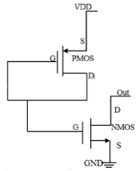
Tie low cells: Initially we directly connect VDD to the gate of transistor now we connect the output of these cells to the gate of the transistor, if any fluctuations in VDD due to ESD (electrostatic discharge) then NMOS circuit pull down it back to the constant low stable state.
in fig the gate and drain of PMOS transistor are shorted and hence this is on saturation region and it acts as pull up resistor and it always gives high voltage to the gate of NMOS transistor and because of this high voltage the NMOS transistor will be ON all the time and we get stable low output because it acts as pull-down transistor and this output is connected to the gate of the transistor.
Tie high cells: Initially we directly connect VDD to the gate of transistor now we connect the output of these cells to the gate of the transistor if any fluctuations in VDD due to ESD then PMOS circuit pull it back to the stable state. PMOS should be ON always, the input of the PMOS transistor is coming from the output of NMOS transistor and here in NMOS gate and drain are shorted and this is the condition of saturation (NMOS) and NMOS will act as pull-down and always give a low voltage at the gate of PMOS. now PMOS will on and gives stable high output and this output is connected to the gate of transistor
 |
| fig: TIE HIGH CELLS |
in fig the gate and drain of PMOS transistor are shorted and hence this is on saturation region and it acts as pull up resistor and it always gives high voltage to the gate of NMOS transistor and because of this high voltage the NMOS transistor will be ON all the time and we get stable low output because it acts as pull-down transistor and this output is connected to the gate of the transistor.
 |
| fig: TIE LOW CELLS |
End cap cells :
- Before placing the standard cells, we can add end cap cells to the block. Endcap cells, which are added to the ends of the cell rows and around the boundaries of objects such as the core area, hard macros, blockages, and voltage areas, and corner cells, which fill the empty space between horizontal and vertical end-cap cells as shown in figure.
- End-cap cells are typically nonlogic cells such as a decoupling capacitor for the power rail. Because the tool accepts any standard cell as an end-cap cell, ensure that you specify suitable end-cap cells.
- Endcap cells placed on the left, right, top, and bottom boundaries, and inside and outside corner cells
- Endcap cells protect your design from external signals.These cells ensure that gaps do not occur between the well and implant layer and to prevent from the DRC violations.
- When you insert these at the end of the placement row, these will make sure that these cells properly integrated to the design and will have a clean unwell, other DRC clean, hence next block will abut without any issues.

No comments:
Post a Comment