Thursday, 24 October 2019

Clock Tree Synthesis


CTS is the process of inserting buffers/inverters along the clock paths to balance the clock delay to all clock inputs. So in order to balance the skew and minimize insertion delay, we are doing CTS.

Inputs for CTS:
  • Detailed placement DB
  • Target for latency and skew , buffers/inverters for building the clock tree
  • Clock Tree DRC (Max Tran, Max Cap, Max Fanout, Max number of levels)

Outputs of CTS:

  • Database with properly build clock tree in the design

Checklist after CTS:

  • Skew Report
  • CLock tree report
  • Timing reports for setup and hold 
  • power and area reports

Why clock routes are given more priority than signal nets?   

Clock is propagated after placement becoz the exact physical location of cells and modules are needed for the clocks propagation which in turn impacts in dealing with accurate delay and operating frequency and clock is propagated before routing becoz when compared to signal routes, clock routes are given more priority. This is becoz clock is the only signal switches frequently which in turn acts as source for dynamic power dissipation.


Difference between clock buffer and normal buffer ?
A buffer is an element which produces an output signal, which is of the same value as the input signal.
Clock buffers are designed specifically to have specific properties that are supposed for clock tree distribution. When compared to normal buffers, clock buffers have
  • equal rise and equal fall times
  • less delays variations with PVT and OCV

Usually in soc’s clock routing is done in higher metal layers as compared to signal routing . So to provide easier access to clock pins from these layers, clock buffers may have pins in higher metal layers. For normal buffers the pins are expected to be in lower metal layers only.
Clock buffers are balanced in other words rise and fall times of clock buffers are nearly equal, the reason behind this is that if the clock buffers are not balanced there will be duty cycle distortion in the clock tree, which can lead to pulse width violations. Compare to normal buffers, clock buffers have high drive strength, due to this it can drive long nets and can have higher fanouts. This help clock buffers and hence to have overall delays.
What is the merits and demerits of clock buffers and clock Inverters ?
Effects of CTS:
  • Clock buffers and clock inverters are added.
  • Congestion and Timing violations may increases
Clock Skew :
  • Keeping clock skew to a minimum is considered to be a good measure of CTS.
  • Clock skew is nothing but difference between 2 flops in arrival times of clock signal at the respective clock pins. 
  • Clock skew = (arrival time at capture clock pin) - (arrival time at launch clock pin)
  • If clock arrival time at capture flipflop is greater than arrival time of launch flipflop , then it is called as positive clock skew. (due to this hold violations occur)
  • If clock arrival time at launch flipflop is greater than arrival time of capture flipflop , then it is called as negative clock skew. (due to this setup violations occur).


    Pre-Placed cells

    PHYSICAL ONLY CELLS

    • These cells are not present in the design netlist. If the name of a cell is not present in the current design, it will consider as physical only cells. they do not appear on timing paths reports, they are typically invented for finishing the chip. 

    fig: TAP Cells and END CAP Cells 

    Tap cells :
    • A tap cell is a special non-logic cell with a well tie, substrate tie, or both. 
    • Tap cells are placed in the regular intervals in standard cell row and distance between two tap cells given in the design rule manual. 
    • These cells are typically used when most or all of the standard cells in the library contain no substrate or well taps.
    • Generally, the design rules specify the maximum distance allowed between every transistor in a standard cell and a well or substrate tap.
    • Before global placement (during the floorplanning stage), you can insert tap cells in the block to form a two-dimensional array structure to ensure that all standard cells placed subsequently comply with the maximum diffusion-to-tap distance limit.
    • Physical only cells which helps to tie substrate and N-Wells to VDD and GND levels, and thus avoids latchup possibiities. 
    What is Latch - up problem ?
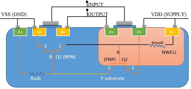
    • It is the condition when low impedance path gets formed between VDD and GND terminal and there is direct current flow from VDD to GND which might result in a complete failure of chip.
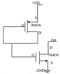
    • While the formation of CMOS INVERTER we saw the formation of PN junctions and because of these PN junctions there may be formation of parasitics elements like diode and transistors. 
    FIG: latch-up phenomenon

    • Transistors Q1(NPN) and Q2(PNP) are parasitics transistors that are getting formed during the manufacturing of CMOS inverter. If these two parasitic transistors are in on condition then current starts flowing from VDD to VSS and creates a short circuit. 
    • While manufacturing these devices the designer made sure that all PN junction should be in reverse bias so that no parasitic transistor will turn on and hence the normal operation will not be affected, but sometimes what happened because of external elements (like input and output) the parasitic transistors get turned on. 
    • For parasitics transistor gets turned on there are two scenarios as discussed below : 
      1. When the input and output > VDD: PNP transistor in ON condition: Because now P region is more positive than N region in Nwell, therefore Base-Emitter junction of PNP (Q2) transistor is in Forward biased and now this transistor will turn on. Now if we see in the fig the collector of PNP transistor is connected to the base of NPN transistor, because of this connection the current is flowing from collector (PNP) to base (NPN) and then because of this base current the NPN transistor gets turn on and the current flowing from VDD to VSS through these two parasitics transistors. This current is flowing even if we removed the external inputs and outputs and parasitic transistors make a feedback path in which current is latched up and creates a short circuit path.
      2. When input and output <VSS: NPN transistor in ON condition: Now N region is more negative than P region in P substrate, therefore Base-Emitter junction of NPN (Q1) transistor is in Forward biased and now this transistor will turn on. Now if we see in the fig the Base of NPN transistor is connected to the Collector of PNP transistor, because of this connection the current is flowing from Base (NPN) to Collector (PNP) and then because of this Collector current the PNP transistor gets turn on and current flowing from VDD to VSS through these two parasitics transistors. This current is flowing even if we removed the external inputs and outputs and parasitic transistors make a feedback path in which current is latched up and creates a short circuit path.
      • In the fig shown above,  the value of Rnwell and Rpsub resistance is quite high, if the values of these resistances will reduced then what will happen? The current flowing from the collector of PNP transistor will flow from these resistance paths, i.e current find the low resistance path to reach from VDD to VSS and NPN transistor will never get turn on and in this way, latchup problem will not occur.
      Solution for latch-up problem:
      • Reducing the resistance values: tap the Nwell to VDD and Psubstrate to GND externally.
      Tie cells:
      • These are special-purpose cells whose output is constant high or low. The input needs to be connected to the gate of the transistor and there are only two types of input logic 1 and logic 0, but we do not connect them directly to gate of the transistor as with supply glitches can damage the transistor so we used tie high and tie low cells (these are nothing but resistors to make sure that PG network connected through them ) and output of these cells are connected to the gate of the transistor.
      • There will be floating nets because of unused inputs they should be tie with some value either low or high to make them stable.
      Why tie cells are inserted?
      • The gate oxide is very thin and it is very sensitive to voltage fluctuations. If the Gate oxide is directly connected to the PG network, the gate oxide of the transistor may get damaged due to voltage fluctuations in the power supply. To overcome this problem tie cells are used.
      How the circuit looks like and how it will work:

      Tie high cells: Initially we directly connect VDD to the gate of transistor now we connect the output of these cells to the gate of the transistor if any fluctuations in VDD due to ESD then PMOS circuit pull it back to the stable state. PMOS should be ON always, the input of the PMOS transistor is coming from the output of NMOS transistor and here in NMOS gate and drain are shorted and this is the condition of saturation (NMOS) and NMOS will act as pull-down and always give a low voltage at the gate of PMOS. now PMOS will on and gives stable high output and this output is connected to the gate of transistor

      fig: TIE HIGH CELLS
      Tie low cells: Initially we directly connect VDD to the gate of transistor now we connect the output of these cells to the gate of the transistor, if any fluctuations in VDD due to ESD (electrostatic discharge) then NMOS circuit pull down it back to the constant low stable state. 
      in fig the gate and drain of PMOS transistor are shorted and hence this is on saturation region and it acts as pull up resistor and it always gives high voltage to the gate of NMOS transistor and because of this high voltage the  NMOS transistor will be ON all the time and we get stable low output because it acts as pull-down transistor and this output is connected to the gate of the transistor.
      fig: TIE LOW CELLS

      End cap cells :
      • Before placing the standard cells, we can add end cap cells to the block. Endcap cells, which are added to the ends of the cell rows and around the boundaries of objects such as the core area, hard macros, blockages, and voltage areas, and corner cells, which fill the empty space between horizontal and vertical end-cap cells as shown in figure.
      • End-cap cells are typically nonlogic cells such as a decoupling capacitor for the power rail. Because the tool accepts any standard cell as an end-cap cell, ensure that you specify suitable end-cap cells.
      • Endcap cells placed on the left, right, top, and bottom boundaries, and inside and outside corner cells
      • Endcap cells protect your design from external signals.These cells ensure that gaps do not occur between the well and implant layer and to prevent from the DRC violations.
      • When you insert these at the end of the placement row, these will make sure that these cells properly integrated to the design and will have a clean unwell, other DRC clean, hence next block will abut without any issues.

      fig: end cap cells


      Placement


      Physical Design Flow


      PHYSICAL DESIGN:

              Physical design means netlist (.v) converted into GDSII form (layout form). In other words logical connectivity of cells converted into physical connectivity.


      IMPORT  :

                  All design related inputs like .v, .libs, .lefs, .sdcs and .upf are read by the tool. After importing all the input files we perform sanity checks like check_design, check_timing to know the netlist related issues. At this stage we need to check that timing is comparable with the synthesis results.

      FLOOR PLANNING :

                 Based on the flylines analysis and hierarchical family, macros are arranged towards the boundary of the design. We also add blockages like soft, hard and partial blockages or density screens to remove the congestion.

      POWER PLANNING :

              Power mesh is build by using the top metal layers on the entire design. Power grid network is created to distribute power to each part of the design equally. Three levels of power distribution
      • Rings : Carries VDD and VSS around the chip
      • Stripes : Carries VDD and VSS from rings across the chip
      • Rails : Connect VDD and VSS to the standard cell VDD and VSS
      Power plan mainly involves placement of :
      • Core power ring
      • Vertical & Horizontal power stripes in the core
      • Standard cells power hookup
      • Block power hookup
      • IO power hookup

      PRE-PLACEMENT :

                  At this stage Well-tap cells and End-cap cells  are inserted in our design.

      PLACEMENT: 

                  Actual placement of standard cells is done. Placement is the process of finding a suitable physical location for each cell in the block. Placement does not just place the standard cell available in the synthesized netlist, it also optimized the design.

      CLOCK TREE SYNTHESIS:

               CTS is the process of connecting the clocks to all clock pin of sequential circuits by using inverter/buffers in order to balance the skew and to minimize the insertion delay. Clock balancing is important for meeting all the design constraints.

      ROUTING:

                  Routing is the actual stage after CTS and optimization where exact paths for interconnection of standard cells and macros and I/O pins are determined.

      Wednesday, 23 October 2019

      PowerPlan VLSI


      Outputs of Physical Design


      Inputs of Physical Design

      PHYSICAL DESIGN :

                      It is the process of transforming netlist into physical layout, which describes the position of cells and routes the interconnection between them.

      Inputs for Physical Design :

      1. Gate level netlist (.v)
      2. Timing, Logical & Power libraries (.lib or .db)
      3. Physical library (.lef)
      4. Technology file (.tf)
      5. TLU + file (.TLUP)
      6. Synopsys Design constraints (.sdc)
      7. Power specification file (.upf or .cpf)

      Name of Inputs

      File  format

      Given by

      Netlist

      .v (Verilog)

      Synthesis team

      SynopsysDesign Constraints  (SDC)

      .sdc(written in TCL)

      Synthesis team

      Timing library / Logical library

      .lib(liberty  file)

      Vendors

      Physical library

      .lef (layout exchange format)

      Vendors

      Technology file 

      .techlef / .tf

      Foundry

      TLU+(Table Look Up)

      .tlup

      Foundry

      Gate level netlist (.v) :

      • Once we synthesize RTL, we will see only gates where connections make the intended logic what we coded in RTL. Since whatever we write in RTL eventually it must be converted to basic gates (no matter how complex algorithm).
      • It contains logical connectivity of all cells (standard cells & macros) and also contains the list of nets (in the design for knowing connectivity by using Fly lines).
      • example of netlist:
        • module and_gate(y,a,b);
        • input a,b;
        • output y;
        • AND2 U1(.Y(y), .A(a), .B(b));
        • endmodule

      Timing, Logical & Power libraries (.lib) :

      • It is generally a .lib/.db file that contains timing & functionality information of all the standard cells, soft macros and hard macros, also design rules like max transition, max capacitance and max fanout.
      • It consists of cell delays, setup and hold in timing information whereas functionality information is used for optimization purpose. 
      • It also contains power information like leakage power for default cell, input and output voltage.
      • PVT corners are also present. for every PVT corner the timing of cells is different. Hence for every PVT corner there is a .lib file present.
      • Cell delay is a function of input transition and output load and is calculated based on lookup tables.
      • Cell delays are calculated by Nonlinear Delay Model(NLDM) and composite current source (CCS) models.
                  

      CCS(Composite current source)

      NLDM (Non-Linear Delay Model)

      It’s like Norton equivalent circuit

      It’s like Thevenin's equivalent circuits

      current source used for driver modeling

      Voltage source used for driver modeling

      It 20 variables to account input transition and output load

      It has only 2 variables.

      CCS is more accurate

      Less accurate

      CCS file is 10x times larger than NLDM because of more numbers of variables

      Smaller than CCS file


      Runtime for CCS is more

      Runtime is less


      Physical library (.lef) :

      • It is a file consists of physical information of standard cells & macros.
        • pin information
      • Height and minimum width of the placement rows.
      • Preferred routing directions
      • Pitch of routing tracks.
      • And also it contains 2 views
        • cell view : useful at the time of tapeout.
        • fram view (abstract view) : useful at the time of place & route.
      • Example of lef:
                                     layer M2
                                     type routing
                                      width 0.50;
                                      end M2
                                      layer via
                                        type cut
                                      end via
                                      macro AND_1
                                            origin 0.000
                                            size 4.5 by 12
                                            symmetry x y;
                                            site core;
                                       pin A 
                                           dir input;
                                            port 
                                            layer M2
                                        end 

      Technology file (.tf) : 

      • It contains name and number convention of metal layer and via information.
      • It contains physical, electrical characteristics & physical design rules of metal layer and via.
      • In physical characteristics:- min width , area, height are present
      • In electrical characteristics:- current density is present
      • Physical design rules like wire to wire spacing, min width between layer and via are present
      • Units and precisions of layer and via
      • Colors and pattern of layer and via

      TLUplus (.tlup) :

      • RC parasitics of metal per unit length. These values are used for calculating net delays.
      • If tlu+ files are not given then these values are taken from .itf file.
      • For loading TLU+ files we have to load 3 files i.e., Max tlu+, Min tlu+ , Map file
      • Map file maps the .ITF file and .tf file of the layer and via names
      • It is a table containing wire cap at different net length and spacing.
      • Milkyway.tf also contain parasitics model of wire as TLU+ contains. If you specify in ICC the TLU+ files then ICC used TLU+ files and did not read parasitics from .tf. if not specified by default ICC will use .tf.
      • Advantage of TLU+ :
        • More accurate
        • Different TLU+ for different RC corners and scenario.
      • Disadvantage of Milkyway.tf : 
        • It is used only for one RC corner.

      Synopsys Design Constraints (.sdc) :

      • Timing constraints like clock definition, timing expections (false paths, multi cycle paths, half cycle paths, disable timing arcs, case analysis & asynchronous paths).
      • Delay constraints like latency, Input delay, Input transition, output load, output transition, min delay and max delay.
      • Power and area constraints
      • Design rule constraints like Max fanout, Max cap & Max transition
      • Clock uncertainity
      • Operating conditions.

      Power specification file (.cpf or .upf) :

      • Power domains or ON/OFF regions
      • PG nets

      FloorPlan VLSI

                  A floorplanning is the process of placing blocks/macros in the chip/core area, thereby determining the routing areas between them. Floorplan determines the size of die and creates wire tracks for placement of standard cells. It creates PG connections. It also determines the I/O pin/pad placement information.
            Before we are going for the floor planning to make sure that the inputs are used for floorplan is prepared properly. After physical design database creation using imported netlist and corresponding library and technology file, steps to done are :  


      1. Decide core width and height for die size estimation.
      2. IO pad sites are created for placement of IO pad placement.
      3. Placement of macros.
      4. The standard cell rows created for standard cell placement.

              Apart from this aspect ratio of the core, utilization of core area, cell orientation and core to IO clearance are also taken care of during the floorplan stage.

      Types of Floorplan Techniques

      • Abutted floorplan : Channel less placement of blocks.
      • Non-Abutted Floorplan : Channel based placement of blocks.
      • Mix of both: partially abutted with some channels.


      Terminologies and Definitions 

      Aspect ratio:  

      • Aspect ratio will decide the size and shape of the chip. It is the ratio between horizontal routing resources to vertical routing resources (or) ratio of height and width.    
        • Aspect ratio = width/height 

      Utilization :

      • Area of the core that is used for placeing Standard Cells and Macros expressed in percentage. core utilization = (macros area + std cell area +pads area)/ total core area

      Manufacturing Grid :

      • The smallest geometry that semiconductor foundry can process or smallest resolution of your technology process (e.g. 0.005)
      • All drawn geometries during Physical Design must snap to this grid
      • While Masking fab. use this as reference lines

      Standard Cell Site/ Standard Cell Placement Tile/ Unit Tile :

      • The minimum Width and Height of a Cell that can occupy in the design
        • The Standard Cell Site will have the same height as Standard Cells, but the width will be as small as our smallest Filler Cell.
      • It’s one Vertical Routing Track and the Standard Cell Height
      • All Standard Cells must be multiple of Unit Tile

      Standard Cell Rows :

      • Rows are actually the Standard Cell Sites abut side by side and then Standard Cells are placed on these Rows
      • Cells with the equal no. of Track definition will have same height

      Placement Grid :

      • Placement Grid is made up of Standard Cell Site
      • Its always a multiple of Manufacturing Grid
      • Placement Grid is made up of the Rows which are composed of Sites

      Routing Grid and Routing Track :

      • Horizontal and Vertical line drawn on the layout area which will guide for making interconnections
      • The Routing Grid is made up of the Routing Tracks
      • Routing Tracks can be Grid-based, Gridless based or Subgrid-based

      Flight-line/ Fly-line :

      • Virtual connection between Macros and Macro or Macros and IOs
      • This helps the designer about the logical connection between macros and pads. 
      • Fly lines act as guidelines to the designer to reduce the interconnect length and routing resources.

      Macro :

      • Any instances other than Standard Cell and is as loaded as black box to the design is Macro.
      • Intellectual Property (IP) e.g. RAM, ROM, PLL, Analog Designs etc.
      • Hard Macro: The circuit is fixed. We can’t see the functionality information about macros. Only we know the timing information. IP with Layout implemented
      • Soft Macro: The circuit is not fixed and we can see the functionality and which type of gates are using inside it. Also we know the timing information. IP without Layout implemented (HDL)
      Guidelines to place macros::

      • Placement of macros are the based on the fly-lines ( its shows the connectivity b/w macro to macro and macro to pins) so we can minimize the interconnect length between IO pins and other cells.
      • Place the macros around to the boundary of the core, leaving some space between macro to core edge so that during optimization this space will be used for buffer/inverter insertion and keeping large areas for placement of standard cells during the placement stage.
      • Macros that are communicating with pins/ports of core place them near to core boundary.
      • Place the macros of same hierarchy together.
      • Keep the sufficient channel between macros. channel width = (number of pins * pitch )/ number of layers either horizontal or  vertical 
      • Avoids notches while placing macros, if anywhere notches is present then use hard blockages in that area.
      • Keep keep-out margin around the four sides of macros so no standard cells will not sit near to Macro pins. This technique avoids the congestion.
      • Keep placement blockages at the corners of macros.
      • For pin side of macros keep larger separation and for non-pin side, we can abut the macros with their halo so that area will be saved and Halo of two macros can abut so that no standard cells are placed in between macros.
      • Between two macros at least one pair of power straps (power and Ground) should be present.
      • Lots of iterations happen to get optimum floorplan, the designer takes care of the design parameter such as power, area, timing and performance during floorplanning.
      Issues arises due to bad Floorplan:

      • Congestion near Macro Pins/ Corners due to insufficient Placement Blockage
      • Std. Cell placement in narrow channels led to Congestion
      • Macros of same partition which are placed far apart can cause Timing Violation

        floorplanning, physical design

      Floorplan Qualification:

      • No I/O ports short
      • All I/O ports should be placed in routing grid
      • All macros in placement grid
      • No macros overlapping
      • Check PG connections (For macros & pre-placed cells only)
      • All the macros should be placed at the boundary
      • There should not be any notches. If unavoidable, proper blockages has to be added
      • Remove all unnecessary placement blockages & routing blockages (which might be put during floor-plan & pre-placing)

      Floorplan outputs

      • IO ports placed
      • cell rows created
      • macro placement final
      • core boundary and area
      • pin position
      • floorplan def


      Important questions related to floorplan :


      1. What are the inputs and outputs for floorplan ?

      Floorplan inputs

      • Technology file
      • Netlist
      • SDC
      • Library files (.lib & .lef)
      • TLU+ file 

      Floorplan outputs

      • IO ports placed
      • cell rows created
      • macro placement final
      • core boundary and area
      • pin position
      • floorplan def

      2. What are the types of floorplan ?


      • Abutted floorplan : Channel less placement of blocks.
      • Non-Abutted Floorplan : Channel based placement of blocks.
      • Mix of both: partially abutted with some channels.
      3. Types of placing standard cell rows?

      4. What are floorplan control parameters ?

      5. What are different steps involved in floorplan?

      6. What are macro guidelines 
      If two communicating macros placed close to each another and if all the pins of both the macros are connected to each other than there is no need of spacing but if some pins are talking with the core logic than we need to provide some spacing so that from the pin route should come and connect to the logic. So minimum spacing required between the 2 macros or boundary and macro is called as the channel.

      7. What is core utilization ?

      It is the ratio of (std cell area + macro area + blockage area) / total area

      8. What is cell utilization ?

      It is the ratio of std cell area/ total area allocated to standard cells

      9. What is gate count?

      Gate count is 3 to 4 times of instance count.
      Total placeable instance area / 2 input NAND gate area in .lib

      10. What is aspect ratio ?

      It is the ratio of vertical routing resources to the horizontal routing resources.

      11. What is a channel ?

      It is the minimum spacing required between two macros or between macros and boundary.

      12. How do you calculate the channel width ?

      Based on the fly-line analysis we will able to know the no. of signals passing through the channel and suppose “21” signals are passing than “21” metal routes are required. So if the signal are need to be routed vertically than we divide the no of routes by no of vertical layers. Suppose no of vertical layers is “3”. On each metal layer 7 track are needed so the width of channel should be equal to 7 tracks.

      13. How do you measure the no. of signals passing through a channel ?

      Through the fly-line analysis

      14. How do you calculate the the metal routes that can be passed through a channel ?

      The no of metal routes required is equal to the no of signal passing through the channel